Introductory nanotechnology
Nanometer (nm) refers to 10-9m. Nanoscience refers to the science concerning the science on the nanoscale. Nanomaterials have size about 1~100nm, they have quite a different properties from normal objects.
Allotropes of carbon
- Diamond has a vast network of tetravalent bonding system, with bond angle 109.5º, the strong covalent allows diamond to have high strength and melting point.
- Graphite forms planar carbon layer with Van Der Waals force holding between layers. As a result they are brittle (layers sliding over each other)
- Carbon nanotubes / fullerene are formed by closed structure of hexagonal/pentagonal rings, they have board uses in medical and other fields.
Properties of nanomaterial
- Mechanical properties like higher tensile strength (maximum stress acting on the solid before it breaks); higher strength without trading off ductility.
- Optically properties like different colours (aqueous nano-sized gold is in red); different behavior in radiation absorption (e.g. ZnO in blocking UV radiation)
- Thermal properties like lower m.p. in smaller size and better thermal conductivity.
- Electrical properties like changing their resistivity (can be increasing / decreasing)
- Magnetic properties like ferromagnetic (magnetization unchanged when permanent magnet is removed) becomes paramagnetic (magnetization disappears when permanent magnet is removes) when the material is in nanoscale.
Reasons behind the different behaviors
- Surface area to volume ratio for nanomaterial is larger. Outsider atoms are usually more reactive then interior atoms. When the surface atoms dominate there can be different properties.
- Quantum effects like the more significant matter wave are given out in nano-sized material and more significant quantization of energy.
Lotus effect
There're many small bumps with wax crystals on the lotus leaf and make it water-repelling. Water on it forms globules and rolls off. This easily catches the dirt, which gives the idea of self-cleaning phenomenon.
Optical Application
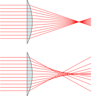
The lenses used in optical microscopes are not ideal. The ideal case is that all parallel light (in different wavelengths) passing through the lens converges at the same point. However in real case there're two aberrations:
Optical aberration: parallel light passing through the lens don't converge at the same point.
Chromatic aberration: light with different wavelengths are bent in different extent by the same lens, causing more than one converging point.
Consider the diffraction of light through a circular small hole. The diffraction patterns are several circular rings with successive bright and dark fringes. When two point sources passes through the hole and diffracts, superposition between two diffractions occurs. Then it may not be able to separate the two patterns (into independent wave functions).
The Rayleigh Criterion states that the image is just resolvable when one's central maximum falls on another's first minimum. When the two wave functions go nearer it's not resolvable.
By calculation we obtain θ≥1.22λ/D, where θ is the intersection angle between two point sources or the angular separation of the two sources. At critical case, θ=1.22λ/D.
Consider the two point sources as the extreme points from a lens. Let s be the separation between two point sources, and f be the focal length. For f>>s, s ≈ fsinθ ≈ fθ = 1.22fλ/D. In practical f > D/2, so s > 1.22fλ/D > 0.61λ. Consider for visible light, λ is about 10-7m, the resolving power of optical instruments are also limited to about 10-7m, so it's impossible to observe nanoscale or smaller scale by optical instruments.
Transmission electron microscopes (TEM)
The electron gun emits electron and accelerated under high potential, and passes through a series of magnetic lens (which bends the electron). It passes through the condensing lens and pass through the object, then pass through objective and projection lens and show the image on fluorescent screen. Since electron has smaller (de Broglie) wavelength, it has higher resolving power. Consider voltage applied as V, energy of electron is V (eV) = mev2/2, then we can calculate the wavelength of the electron beam. It's also acceptable that the de Broglie wavelength is approximately equal to the resolving power of the microscope.)
Scanning Tunnelling microscopes (STM)
The tip of the microscopes is about the size of several atoms. They kept a short distance from the object (several nm). A small positive potential is given to the tip so that tunnelling current is produce between the object and the tip. As explained before the tunnelling current is related to the distance between the tip and the object, then the 3D structure of the object is scanned.
Applications
- Controlling individual atoms, CPU production
- Nanomaterials with specified properties like medicine, ductile ceramics, clothes…
- Photocatalysts which enables functions (like dirtiness prevention, anti-fog, anti-bacteria, water treatment and deodorization) under the presence of light like TiO2 and ZnO
- Nanotechnology like solar panel using nanomaterials and robots.
Potential Hazards
- Nanomaterials are reactive than its bulk form, and is more volatile, soluble and penetrating, so it can be more easily to be absorbed and can be more toxic.
- They may have unknown toxicity or even causing DNA mutations
- Polluting the environment and cause social problems (e.g., upraise of nanoweapons)


No comments:
Post a Comment